Page 14 of 43
Re: Couldnt really find a section for this..
Posted: Tue Aug 02, 2011 9:59 pm
by The1
grab this pdf has labels and pinouts for the 24c44
http://www.google.com.au/url?sa=t&sourc ... 5620ZhXi_w
then you want to look at the schematic for the 93x in that pdf
Otherwise easy version
The ICSP header on the programmer has pins 1-10
So chip to programmer
1-3
2-4
3-5
4-6
5-10
6,7,8-1
Re: Couldnt really find a section for this..
Posted: Tue Aug 02, 2011 10:01 pm
by festy
The1 wrote:
64^A8^00 = CC ^ FF = 33 So CC 33 which is how i did the ones that worked
Don't worry about changing word 0, just keep the first 4 words as they are

If you work in native byte order, it makes life a whole lot easier.
That way 1526 would be 00FF 15EA 26D9. 00+15+26=3B. 3B^FF = C4.
So that block would be C43B 00FF 15EA 26D9.
Convert to LSB for your burner if you need to, and you're away.
Re: Couldnt really find a section for this..
Posted: Tue Aug 02, 2011 10:02 pm
by Streetholden
Ah i think i understand, Cheers. Ill wait till i have the programer in my hands before i ask anything else as generally its easier when its infront of you.
Re: Couldnt really find a section for this..
Posted: Tue Aug 02, 2011 10:25 pm
by festy
The1 wrote:
This is what i made up
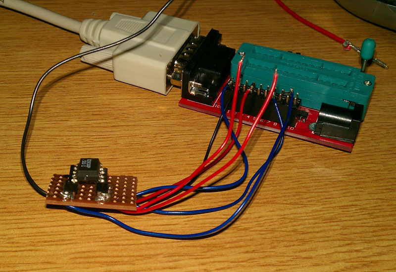
That adapter is almost as complex as my whole programmer

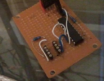
- pic.jpg (18.51 KiB) Viewed 5311 times
Re: Couldnt really find a section for this..
Posted: Tue Aug 02, 2011 11:01 pm
by The1
festy wrote:The1 wrote:
64^A8^00 = CC ^ FF = 33 So CC 33 which is how i did the ones that worked
Don't worry about changing word 0, just keep the first 4 words as they are
If you work in native byte order, it makes life a whole lot easier.
That way 1526 would be 00FF 15EA 26D9. 00+15+26=3B. 3B^FF = C4.
So that block would be C43B 00FF 15EA 26D9.
Convert to LSB for your burner if you need to, and you're away.
yeh tried that way to, not working on my VS dash, some work some dont driving me mental
Re: Couldnt really find a section for this..
Posted: Tue Aug 02, 2011 11:08 pm
by festy
Are you xoring, or adding?
Re: Couldnt really find a section for this..
Posted: Tue Aug 02, 2011 11:14 pm
by The1
tried both, i even just copied your line above

ive tried quite a few combinations, it seems that i can see any numbers above 1's or 10's and they so far all work, but some numbers in the 1's and 10's dont
Re: Couldnt really find a section for this..
Posted: Wed Aug 03, 2011 12:13 am
by The1
like this for me

1520KM
works
AC53 FF00 57A8 FB04
8A40 = 1520
A8+04=AC^FF=53
doesn't work
CA35 FF00 15EA 20DF
00+15+20=35^FF=CA
Re: Couldnt really find a section for this..
Posted: Wed Aug 03, 2011 6:47 am
by festy
The1 wrote:
doesn't work
CA35 FF00 15EA 20DF
00+15+20=35^FF=CA
You need to convert to LSB so your programmer can read the bin correctly - the line above is still MSB.
Re: Couldnt really find a section for this..
Posted: Wed Aug 03, 2011 9:04 am
by festy
Com port code done and working, I now have a functioning programmer

Just a bit more pcb tracing to do and I should have programming via the dash's CN103 connector under way.
The 24C44's CE line is handled by one of the inverting schmitt triggers - the track runs under the 74HC14 but assume it's the one that runs back to the connector.
I have been trying to work out how the 8051 gets told to shut up during programming - if it was talking on the SPI lines while you're programming, the data would get garbled.
But I'm hoping that the mcu copies the 'c44 ram to it's own internal ram, and only talks to the external storage for updates after that - which would mean that as long as there were no vss pulses coming in, the spi lines would be quiet.
Actually, I can test this with my dodgy soundcard-scope - if I'm right, the sclk line will be silent after the initial read on power-up ...
edit: Yep, looks like the mcu only does an initial read on power-up, so shouldn't interfere with programming the nvram.