Page 4 of 6
Re: P59 flash kernel development
Posted: Thu Jan 02, 2020 5:39 am
by Gampy
Whoo Hoo ... Another brick OFF the wall!
BDM works great!
In case any body wants the pin outs.
Code: Select all
 A-4  = GND    -> Pin 3
 A-7  = DS     -> Pin 1
 A-11 = DSI    -> Pin 8
 A-13 = DSO    -> Pin 10

 B-12 = BERR   -> Pin 2

 C-12 = RST    -> Pin 7
 C-29 = DSCLK  -> Pin 4
 C-30 = Freeze -> Pin 6
The Intel chip also requires +12v on WPP during Write, I do not have the location of WPP yet.
Oh what a relief it is!
Re: P59 flash kernel development
Posted: Thu Jan 02, 2020 5:48 am
by DavidBraley
Gampy wrote:I do not have the location of WPP yet.
Actually, you do. Look at the cad file I sent you. It's also in the images you stripped the meta data from.
Re: P59 flash kernel development
Posted: Thu Jan 02, 2020 6:26 am
by Gampy
DavidBraley wrote:Gampy wrote:I do not have the location of WPP yet.
Actually, you do. Look at the cad file I sent you. It's also in the images you stripped the meta data from.
I saw no locations in the images at all ... I'm talking about the locations silk screened on the board.
Whoops Sorry, Have not looked at the CAD file yet, maybe my bad ...
Re: P59 flash kernel development
Posted: Thu Jan 02, 2020 7:42 am
by DavidBraley
Gampy wrote:DavidBraley wrote:Gampy wrote:I do not have the location of WPP yet.
Actually, you do. Look at the cad file I sent you. It's also in the images you stripped the meta data from.
I saw no locations in the images at all ... I'm talking about the locations silk screened on the board.
Whoops Sorry, Have not looked at the CAD file yet, maybe my bad ...
It's this image:
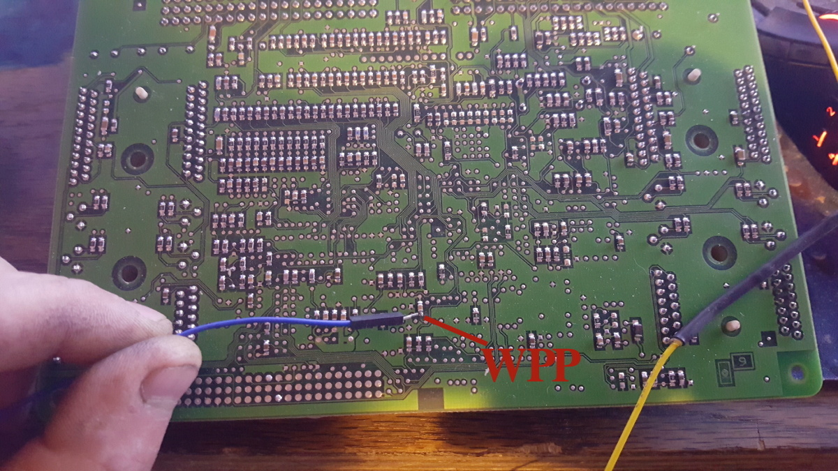
- BackSideWPP.jpg (777.39 KiB) Viewed 3634 times
Re: P59 flash kernel development
Posted: Thu Jan 02, 2020 7:53 am
by DavidBraley
Gampy,
Do not apply anything less than 11.4 Volts, and no more than 12.6 Volts to the WPP pin. This info is from the Intel flash datasheet.
Re: P59 flash kernel development
Posted: Thu Jan 02, 2020 9:28 am
by Gampy
DavidBraley wrote:Gampy wrote:DavidBraley wrote:
Actually, you do. Look at the cad file I sent you. It's also in the images you stripped the meta data from.
I saw no locations in the images at all ... I'm talking about the locations silk screened on the board.
It's this image:
I see no Silk Screened locations in that image.
[edit added image]
Like this,
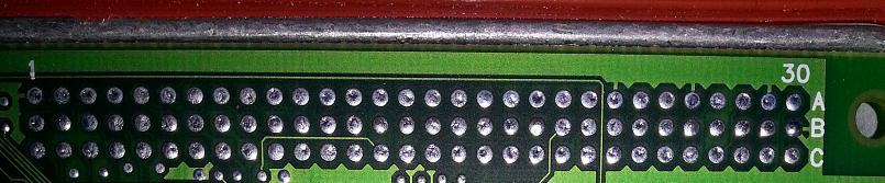
- 90PinDiagnosticsHeader.JPG (37.37 KiB) Viewed 3627 times
1, 30, A, B, C
Thank you for the voltage warning.
Re: P59 flash kernel development
Posted: Thu Jan 02, 2020 10:47 am
by DavidBraley
I'm not understanding you when you say "silk screened locations."
The location you apply the 12 volts erase and write voltage to the Intel Flash chip (what the BDM calls WPP) is not on the 90 pin header. It's where the red and black arrows are pointing (the second close-up image only has a black arrow). Sorry about the blurry images. If you view the cad file I sent you, it will all make more sense. I hope this helps!

- WPP_Pin.jpg (978.54 KiB) Viewed 3624 times

- wppsmall.jpg (1.04 MiB) Viewed 3624 times
Re: P59 flash kernel development
Posted: Thu Jan 02, 2020 11:27 am
by DavidBraley
OK, now I understand what you mean by "silk screened locations." I'm slow sometimes...
Re: P59 flash kernel development
Posted: Thu Jan 02, 2020 12:07 pm
by Gampy
Bah humbug, it looks like there is nothing around to textually describe it's location.
Thanks David
Re: P59 flash kernel development
Posted: Thu Jan 02, 2020 1:52 pm
by Vampyre
david can i get that cad file please